Product Overview
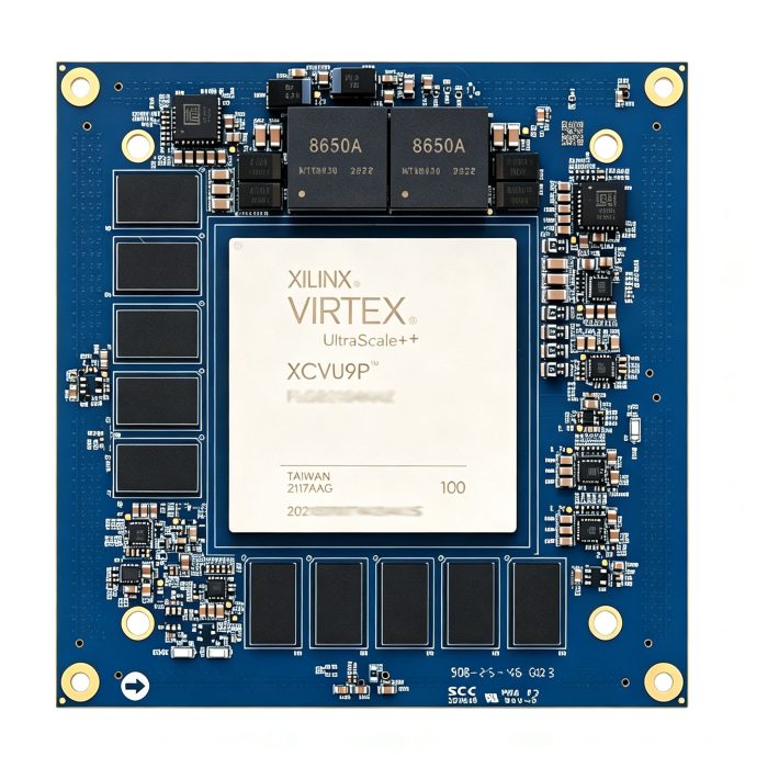
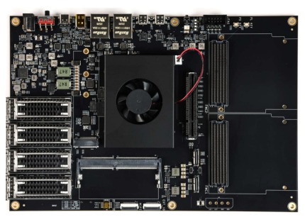
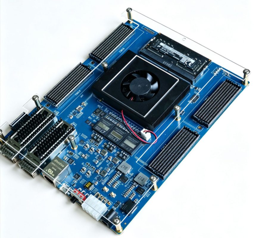
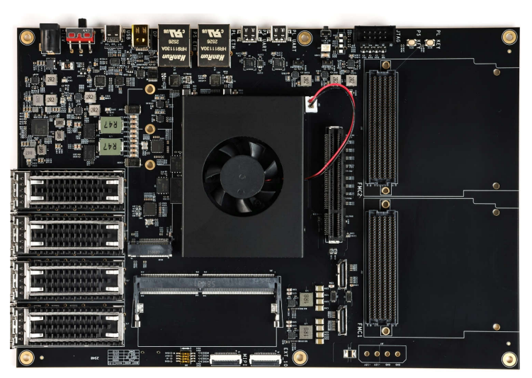
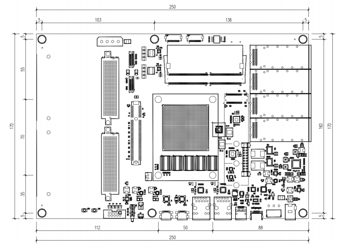
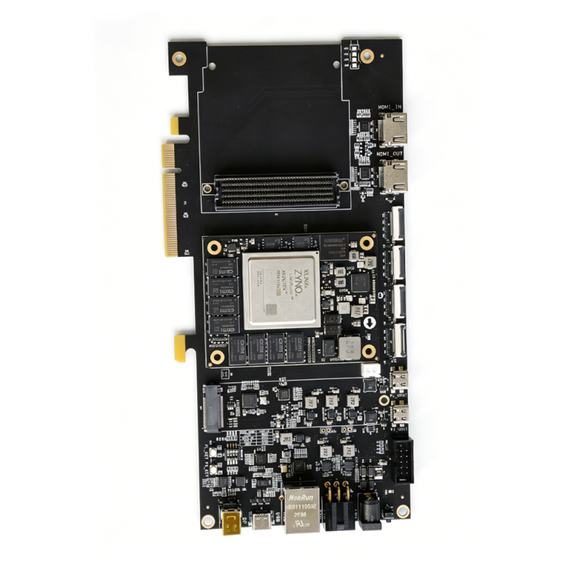
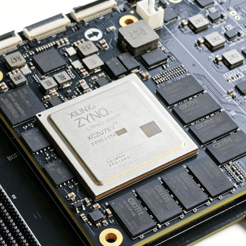
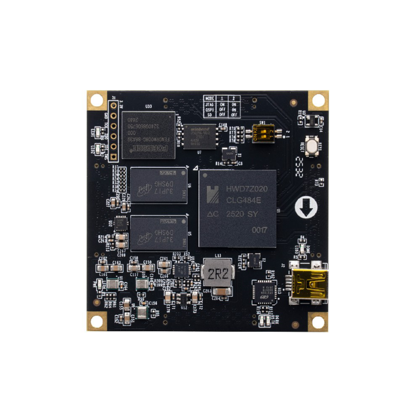
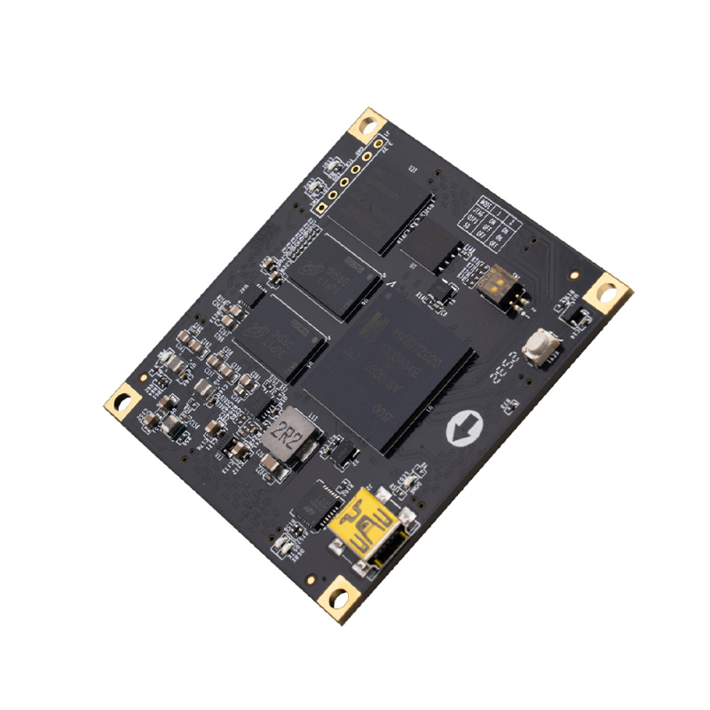
VU9C (XCVU9P) Compute Edition ultra-high-end development board, designed based on AMD Xilinx Virtex UltraScale+ industrial-grade FPGA chip XCVU9P-2FLGB2104, capable of stable operation in the -40°C~85°C temperature range. The board adopts a core board + baseboard separation architecture (core board 106×106mm / baseboard 210×255mm), equipped with massive logic resources, abundant DSP computing units, large-capacity on-chip memory, and multiple high-speed optical ports/PCIe interfaces, targeting high-computing, high-bandwidth application scenarios such as high-speed networking, ASIC prototyping verification, high-performance computing, and real-time signal processing.
Key Highlights
- Flagship Computing Power: Equipped with 2,586K logic cells and 6,840 DSP slices, supporting ultra-large-scale parallel computing;
- Ultra-Large On-Chip Cache: 75.9Mb BRAM paired with 270Mb UltraRAM, achieving ultra-low-latency data interaction;
- Extreme Interconnect Capability: Equipped with PCIe Gen3 ×16 gold finger, 2×QSFP-DD + 4×QSFP28 high-speed optical ports, dual FMC (FMC+/HPC) and M.2 NVMe, fully unleashing bandwidth performance;
- Large-Capacity Memory Configuration: Onboard 32GB DDR4 ECC (4×72bit), capable of handling massive data throughput;
- High-Precision Clock: Onboard Si5341 clock tree + TCXO, supporting 10MHz / 1PPS external reference synchronization;
- Industrial-Grade Reliability: Wide-temperature hardware design, 12V/20A power supply with PMBus telemetry support, capable of long-term operation in harsh industrial environments.
Applications
ASIC Prototyping & Functional Verification
Leveraging 2,586K ultra-large logic cells, thousands of DSP computing power, and large-capacity on-chip UltraRAM cache, it can fully replicate the logic architecture of large-scale ASIC/SoC chips, supporting early prototyping verification and functional simulation of complex digital circuits, AI operators, and communication protocol chips, significantly shortening the tape-out cycle of high-end chips and reducing R&D trial-and-error costs.
High-Speed Communications
Suitable for high-end communication scenarios such as 5G/6G base station BBU baseband processing, fronthaul/backhaul optical transmission, and 400G/800G data center high-speed switching. Onboard 2×QSFP-DD + 4×QSFP28 high-speed optical ports support parallel modulation/demodulation, channel coding/decoding, and protocol stack hardware acceleration for multiple high-speed data streams.
High-Performance Computing & AI Inference
Based on PCIe Gen3 ×16 high-bandwidth interface and 32GB DDR4 ECC large memory, it can connect to servers for AI model inference, high-frequency trading, real-time signal processing, and other low-latency, high-throughput applications, offering lower latency and higher throughput compared to general-purpose CPUs.
High-Precision Measurement & Testing
Onboard Si5341 + TCXO high-precision clock and SMA trigger/clock interfaces, suitable for radar, electronic countermeasures, high-speed data acquisition, and test measurement applications with stringent latency and synchronization requirements.

Reviews
There are no reviews yet.